

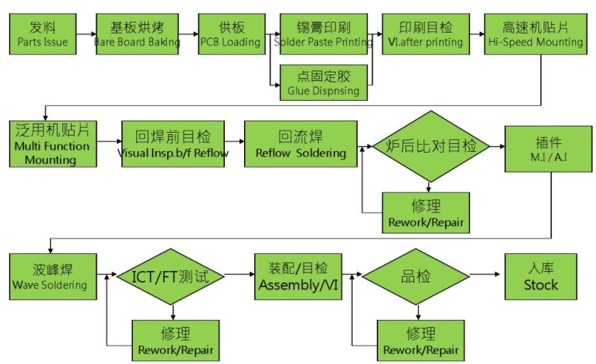
While SMT has become the mainstream in PCBA manufacturing, the DIP (Dual In-line Package) insertion process remains indispensable in certain applications due to its high reliability, strong mechanical connections, and compatibility with large/high-power components. Today, let’s break down the complete DIP insertion workflow to better understand this traditional yet critical technology.
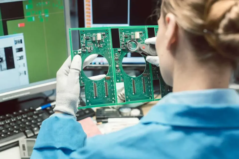
1. Incoming Inspection
Component Check: Ensure no pin oxidation and verify BOM against physical components.
PCB Check: Confirm pad integrity and hole diameter compliance.
Preparation: Adjust component pin spacing; some may require pre-cutting for easier insertion.
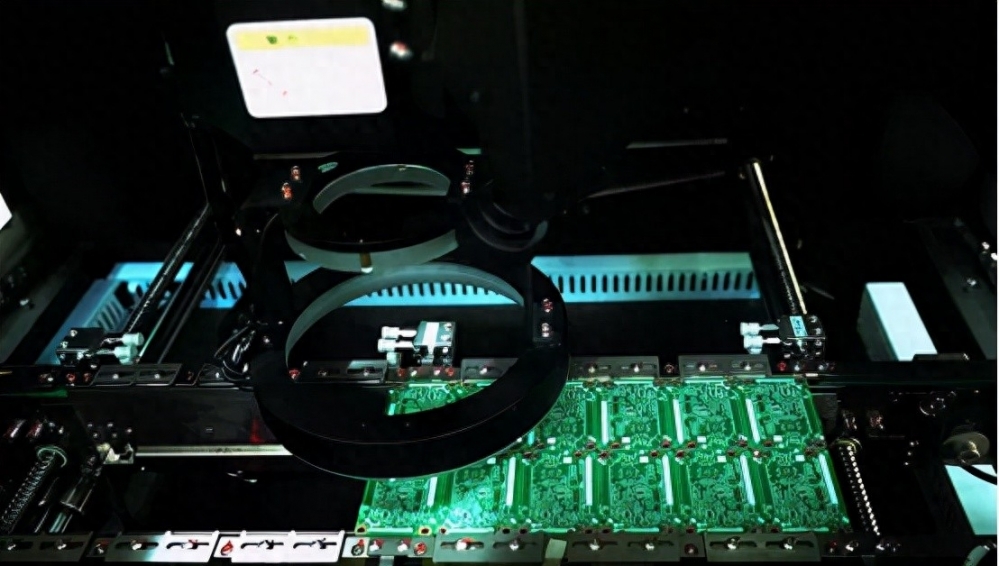
2. Component Insertion
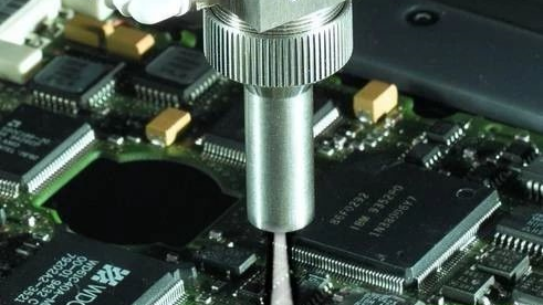
Manual Insertion: Used for low-volume, complex, or large components.
Automated Insertion: High-speed machines for standard components (e.g., resistors, capacitors), ideal for mass production.
3. Wave Soldering
Preheating → Flux Application → Wave Soldering (250-270°C) → Cooling
Key parameters: Conveyor speed, wave height, and temperature to ensure strong, defect-free solder joints.
4. Post-Soldering Inspection
Visual Inspection: Check for solder joint integrity, shorts, or cold joints.
AOI (Automated Optical Inspection): Scan for defects and mark faulty points.
X-ray Inspection: For hidden joints or high-density boards.
Functional Testing: Verify electrical performance under simulated operating conditions.
5. Cleaning, Protection & Packaging
Cleaning: Remove flux residues for better PCB cleanliness.
Conformal Coating (if needed): Protects against moisture and corrosion in harsh environments.
Final Packaging: After quality approval, boards are packed for delivery.
Though DIP involves more steps than SMT, its durability and reliability keep it essential in industries like industrial control, power modules, and automotive electronics.
What’s your experience with DIP assembly? Share your thoughts in the comments!

 whatsapp