

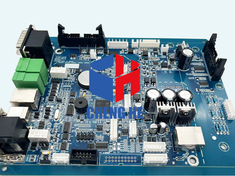

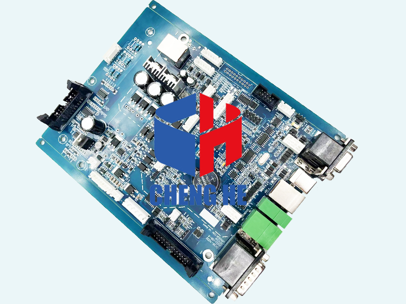
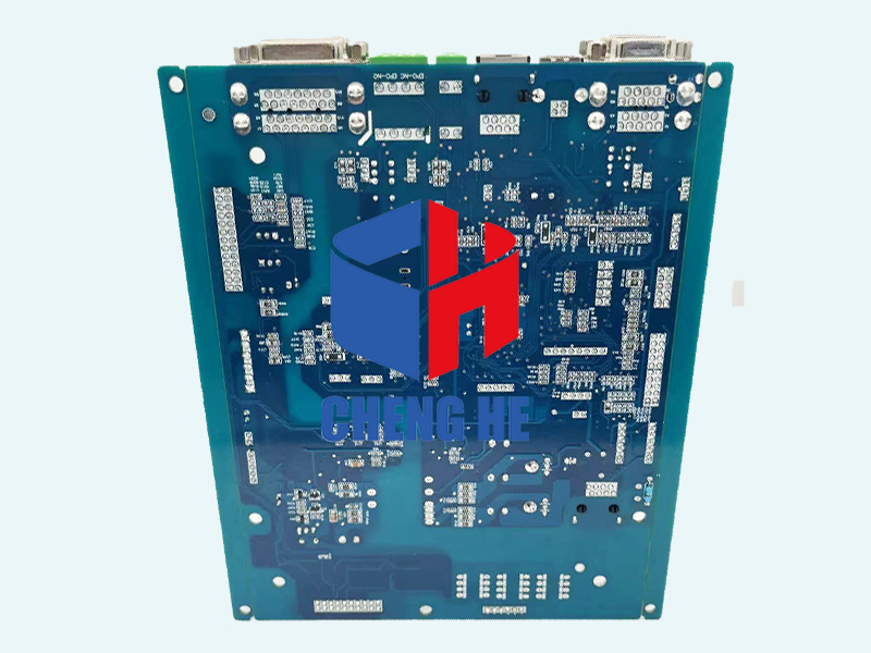
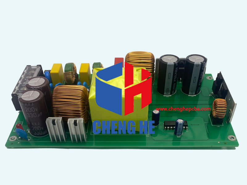
Material: | FR4 | Layer: | 6L |
Board thickness: | 2.0mm | Min Hole: | 0.2MM |
Copper thickness: | 3OZ | Solder mask: | Blue |
Min Width & Space: | 5mil/5mil | Silkscreen: | White |
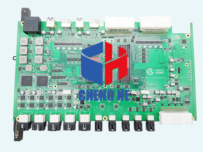
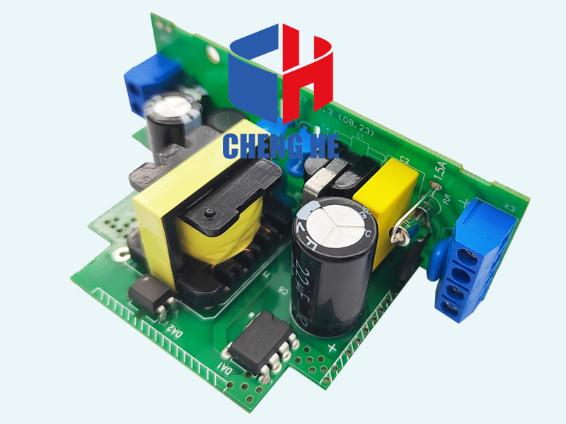
Finishing: | HAL LF | Application: | Power supply PCBA |
Special: | Thick copper | ||
What are the highspeed layout design rules?
While designing a circuit board for high-speed applications, strongly focus on the layout. The layout design rules mentioned below will not only fulfill the design requisites but will also reduce the manufacturing cost.
1. Place a common ground plane below the signal traces.
This ensures minimal impedance between any two ground points in the board. The ground plane should never be broken by routing any tracks in it.
2. Using split ground planes reduces the noise in analog ground planes.
While using split ground planes, it is mandatory to route all the traces going from one region to the other exclusively above the interconnecting point.
3. Place signal vias properly.
Improper positioning of vias can create plane areas in which the current density is increased. It is better to place vias forming a grid, it leaves enough space between the vias to incorporate the power plane (place them 15 mils apart).

 whatsapp