

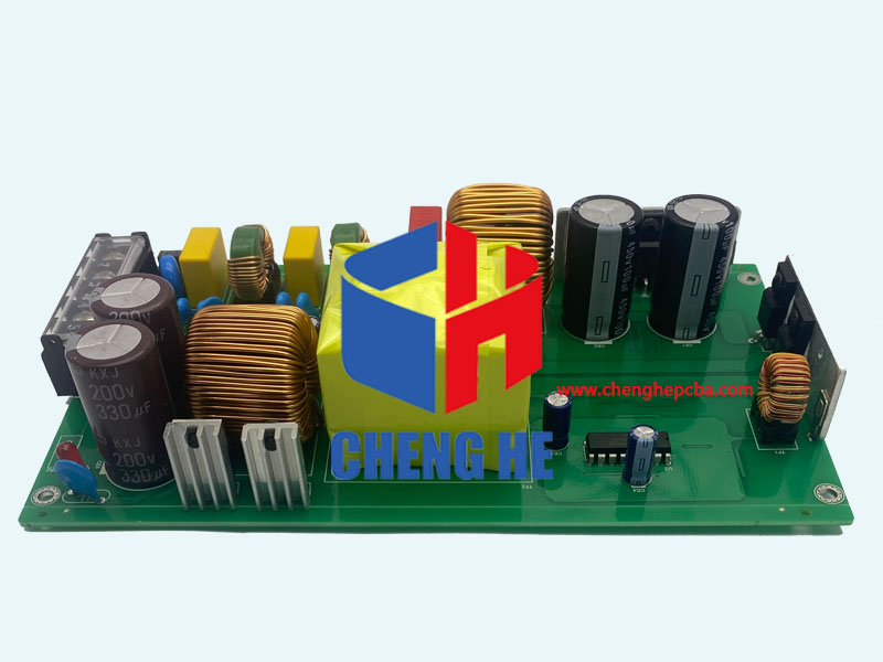
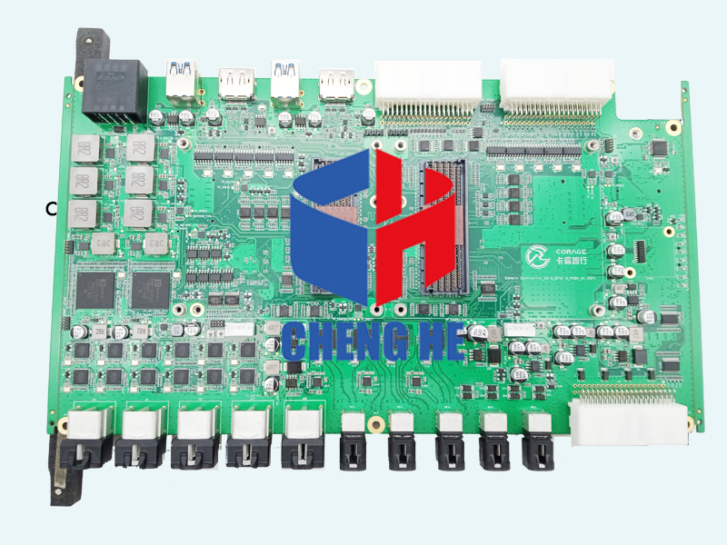
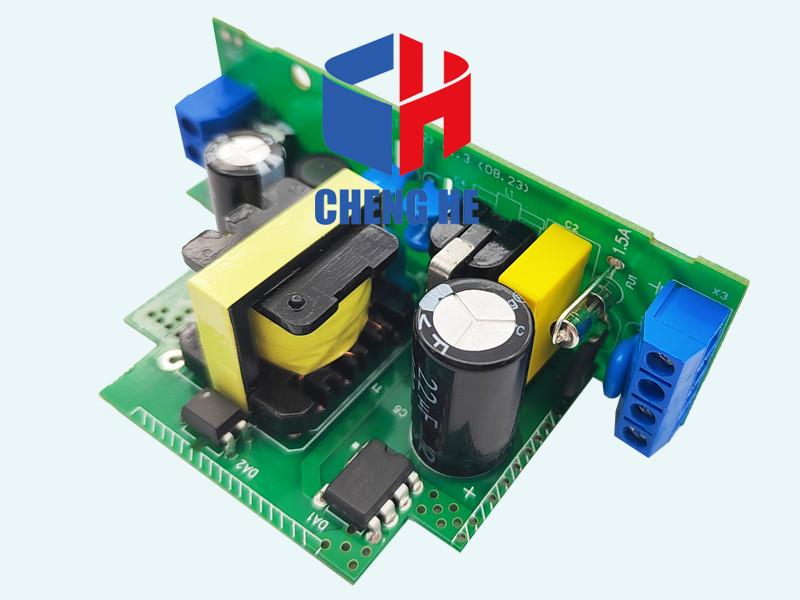
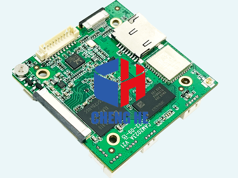
Material: | FR4 | Layer: | 2L |
Board thickness: | 1.6mm | Min Hole: | 0.25mm |
Copper thickness: | 1 OZ | Solder mask: | Blue |
Min Width & Space: | 0.2mm/0.25mm | Silkscreen: | White |
Finishing: | ENIG 2u" | Application: | LED signal |
Special: | |||
PCB common IC packaging
1. SOT: General Pin is less than 5 small shape transistors
2. SOP: Small shape bilateral surface mount package
3. PQFP: Applicable high-frequency circuit, the distance between the chip pin is small, generally large-scale integrated circuits adopted
4. PLCC: The pin is taken from the four sides of the package, which is j-shaped, the J-pin is not easy to deform, but the appearance inspection after welding is difficult
5. QFN: The four sides of the package are configured with electrode contacts, no foot flat packages.
6. BGA: The bottom is the array spherical bump, the electric thermal performance is good, the signal transmission is delayed, and the reliability is high.
7. PGA: Pin grid array package, generally connected to the PCB board through the socket.
8. DIP: Double column inserted package
9. SIP: single-column insert package

 whatsapp