

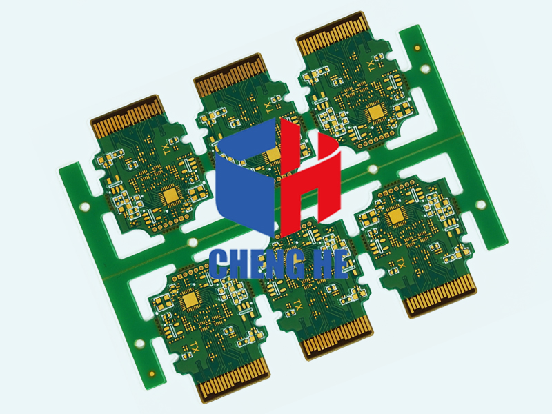
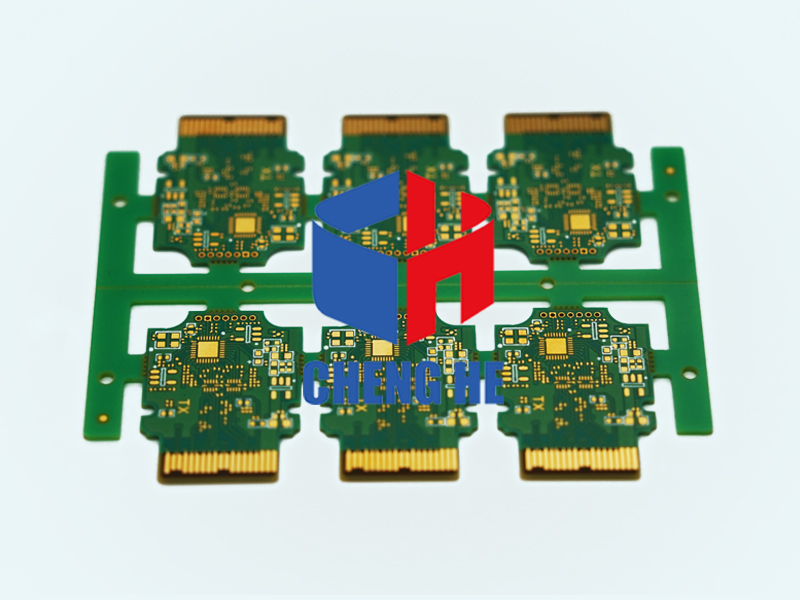
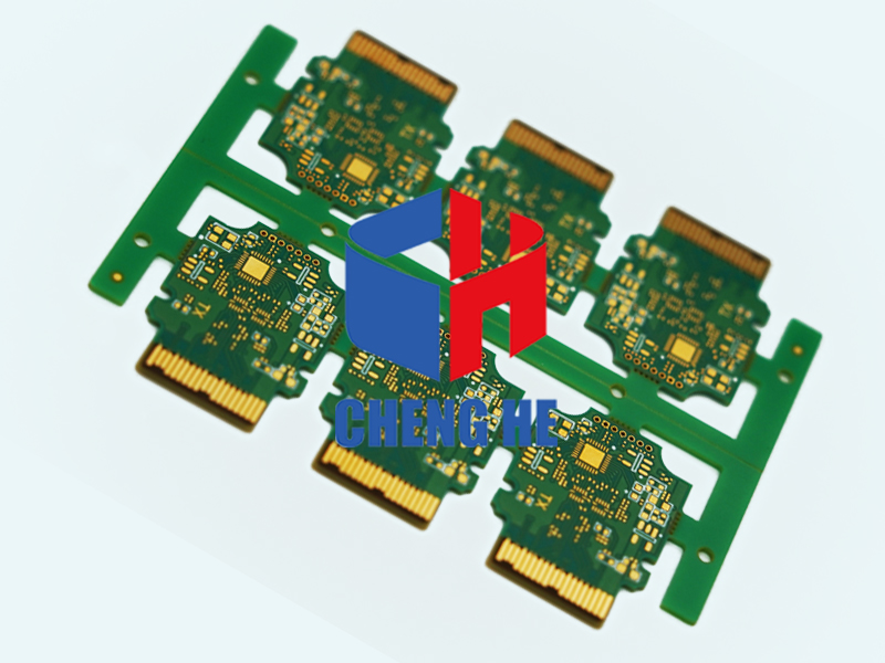

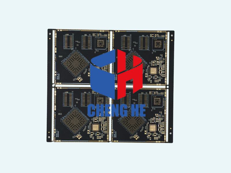
Material: | FR4 | Layer: | 4L |
Board thickness: | 1.6mm | Min Hole: | 0.2MM |
Copper thickness: | 1OZ | Solder mask: | Green |
Min Width & Space: | 6mil/6mil | Silkscreen: | White |
Finishing: | ENIG+Gold finger | Application: | Optical module |
Special: | High gold finer requirement 20U” | ||
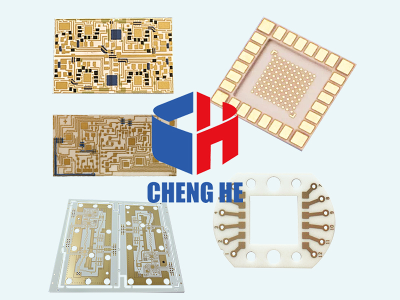
Gold fingers are the gold-plated columns that you see along the connecting edges of printed circuit boards (PCBs). The purpose of gold fingers is to connect a secondary PCB to the motherboard of a computer. PCB gold fingers are also used in various other devices that communicate via digital signals, such as consumer smartphones and smartwatches. Gold is used for the connecting points along a PCB because of the alloy’s superior conductivity.
There are two types of gold applicable to the PCB gold finger plating process:
· Electroless Nickel Immersion Gold (ENIG): This gold is more cost-effective and easier to solder than electroplated gold, but its soft, thin (typically 2-5u” composition renders ENIG unsuitable for the abrasive effects of circuit board insertion and removal.
· Electroplated Hard gold: This gold is solid (hard) and thick (typically 30u”), thus more ideal for the abrasive effects of constant PCB usage.
Gold fingers make it possible for different circuit boards to communicate with one another. From the power source to the device or equipment, signals must pass between several contacts for a given command to be enacted.
Once you press a command, the signal will pass between one or more circuit boards before it is read. For example, if you press a remote command on a mobile device, the signal will be sent from the PCB-enabled device in your hand to the near or distant machine, which in turn receives the signal with its own circuit board.
The process involved in the plating of gold fingers involves a number of meticulous steps. This ensures each circuit board rolling off the production line is properly equipped to conduct signals free of error. The standards involved in the plating process also helps to ensure a perfect fit between the gold fingers on each circuit board with the corresponding slots on a given motherboard.
To ensure that all of these fingers and slots fit hand-in-glove, each PCB must pass a series of inspections and defect tests. If the gold plating on a circuit board lacks smoothness or does not adequately adhere to the surface, the results will not be sufficient for commercial release.

 whatsapp